












Unprecedented bandwidth demands require a fundamental rethinking of the optical interconnection roadmap, bringing optics closer to silicon chips.
The explosive growth of cloud computing and AI – from generative and inferential approaches to ultimate agent systems – is generating unprecedented demands for bandwidth, as the volume of data that needs to be transmitted both within and between data centers continues to surge. At the same time, this also exposes the limitations of the underlying interconnects, which extend not only across data center networks and rack levels but also deep into the servers themselves, reaching the level of packaging and chips, to connect XPU, memory, and other system components.
For a long time, copper-based electrical interconnects have been the industry standard due to their low cost, simplicity, and reliability. However, nowadays they are approaching fundamental limitations: although they can achieve high-energy-efficiency electrical connections, they are typically only suitable for very short distances (on the order of millimeters). At longer distances and higher channel speeds, power consumption increases sharply, thermal constraints become more severe, and signal integrity declines. In other words, electrical I/O is rapidly becoming a key obstacle to the expansion of next-generation AI and machine learning systems.
Optical interconnection has become a key direction for advancement. By transmitting data using light rather than electrical signals, optical interconnection is much less sensitive to distance, which can significantly improve energy efficiency while alleviating the inherent crosstalk and thermal issues of copper interconnections. However, even optical technology is now being pushed to new limits due to industry demands for (multi-)terabits per second interfaces, ultra-high energy efficiency, and extremely low (sub-microsecond) latency.
Meeting these requirements cannot be achieved solely through incremental innovation. This requires a fundamental rethinking of the optical interconnection roadmap; that is, to gradually move optics from the front panel to within the package and ultimately to integrate it firmly into the wafer stack.
Pluggable optical module ( PO ): A leading solution that has been active for a long time and remains so to this day.
For over two decades, pluggable optical transceivers have been a cornerstone of high-speed telecommunications and data communication networks – from enterprise workloads and video streaming media to today's ultra-large-scale cloud infrastructure, none of which can function without them. Pluggable modules are inserted into standardized ports on switches, routers, and servers, converting the electrical signals from the host into optical signals for transmission over fiber optic cables, and then converting them back at the receiving end.
The advantages they bring include:
- Modularity and flexibility – the optical components can be upgraded independently of the electrical main unit.
- Maintainability – Plug-and-play modules support hot swapping, allowing for replacement without the need to shut down the system.
- Multi-vendor interoperability is achieved through the IEEE 802.3 standard, as well as widely adopted multi-source protocols such as QSFP, QSFP-DD, and OSFP ( MSA ) physical specifications.
- Thermal stability – The light engine is located in the front panel cage, physically isolated from high-power ASIC components; this helps to protect the laser, modulator, and photodetector from overheating, thereby enhancing reliability.
Over several generations of products, pluggable optical transceivers have evolved from 100/200G to 400G and 800G by increasing the baud rate (the number of symbols transmitted per second per optical channel), adopting higher-order modulation (such as PAM-4), and increasing the number of parallel channels.
Although the technology is already quite mature, pluggable optical modules continue to evolve. For example, the first-generation 1.6T pluggable transceivers—relying on a data rate of 200Gbps per channel and utilizing an eight-channel parallel architecture—are approaching the sample and early deployment phases. The target applications include direct connections within data centers ( DR ) as well as forward coverage ( FR ) connections achieved through single-mode fiber optics.
The key driving factor is silicon photonics ( SiPho ), which supports this expansion through a series of optical and electronic components based on silicon, including the Mach-Zehnder modulator. Such devices are capable of operating at 200 Gbps per channel in a cost-effective manner while maintaining controllable power consumption.
Looking further into the future, by the end of this decade, the industry is aiming for a milestone of 3.2T pluggable optical modules. However, to achieve these performance levels, continued progress in high-speed electronics, packaging, and thermal management is required, as well as a significant expansion of the silicon photonics toolkit. Taking the transmitter side as an example, optical modulators will need to support bandwidths exceeding 100GHz while maintaining low insertion losses and high modulation efficiency – requirements that are becoming increasingly difficult to meet with traditional silicon devices alone.
Figure 1: Over the past few years, pluggable optical modules have achieved order-of-magnitude improvements in both bandwidth density and energy efficiency. Source: imec.
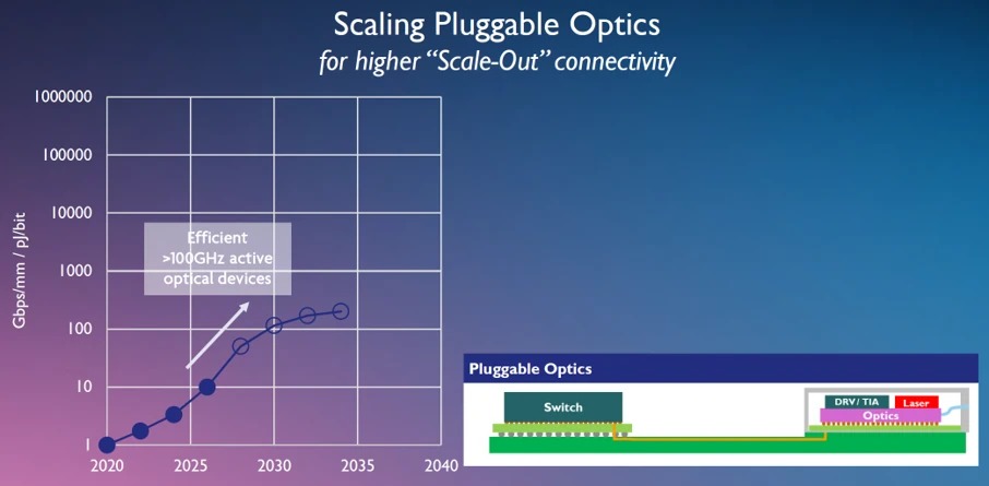
In response to these limitations, the industry has begun to focus on the integration of higher-performance electro-optical materials with heterogeneous properties, such as lithium niobate ( LiNbO₃ ) and lithium tantalate ( LiTaO₃ ). Technologies like micro-transfer printing offer promising avenues for integrating these materials onto silicon photonic platforms. Early results are encouraging, but further research is still needed to scale these methods for mass production. This is essential so that future 3.2T modules can not only be practical and reliable but also maintain the cost-effectiveness that makes pluggable optical modules the mainstream in the industry.
At the same time, other expansion paths are also under exploration. Concepts such as the ultimate pluggable optical module ( XPO ) attempt to increase bandwidth density further, raising capacity to 12.8T, but the trade-off is a significant increase in system complexity, and liquid cooling is required. This will at least affect costs and practical deployment for now.
Double World's first: Integrating LiNbO₃ and LiTaO₢ onto SiPho through micro-transfer
As optical interconnects are required to break through the current standard of 200 Gbps per channel, devices based on GeSi are becoming increasingly unable to provide the desired combination of bandwidth and energy efficiency simultaneously. Although GeSi modulators have achieved 400 Gbps per channel in the C-band, this level has not yet been reached in the O-band. To unleash the next performance leap in pluggable optical interconnects, researchers are exploring the heterogeneous integration of advanced electro-optical materials such as lithium niobate ( LiNbO₃) and lithium tantalate ( LiTaO₃) onto silicon photonic devices, paving the way for a new generation of high-speed modulators and photodetectors.
A very promising implementation method is micro-transfer printing, which can precisely place thin film materials onto SiPho wafers, without the material waste, post-bonding complexity, and costs associated with traditional wafer bonding. Two world-first achievements demonstrate its potential:
Firstly, researchers from imec and the University of Ghent demonstrated an unamplified optical link at the O-band with a speed of 320 Gbps over a transmission distance of 2 kilometers using single-mode fiber. This achievement utilized high-bandwidth 100 GHz germanium photodiodes, combined with transferred thin-film lithium niobate Mach-Zehnder modulators (MZM), which were integrated into a SiPho platform. These modulators were also packaged together with custom traveling-wave drivers and TIA. This work marks the first time that LiNbO 3 modulators have been seamlessly integrated into a silicon photonics platform through microtransfer.
Figure 2: For the first time, the LiNbO 3 modulator is seamlessly integrated into the silicon photonics platform through micro-transfer. Source: imec.
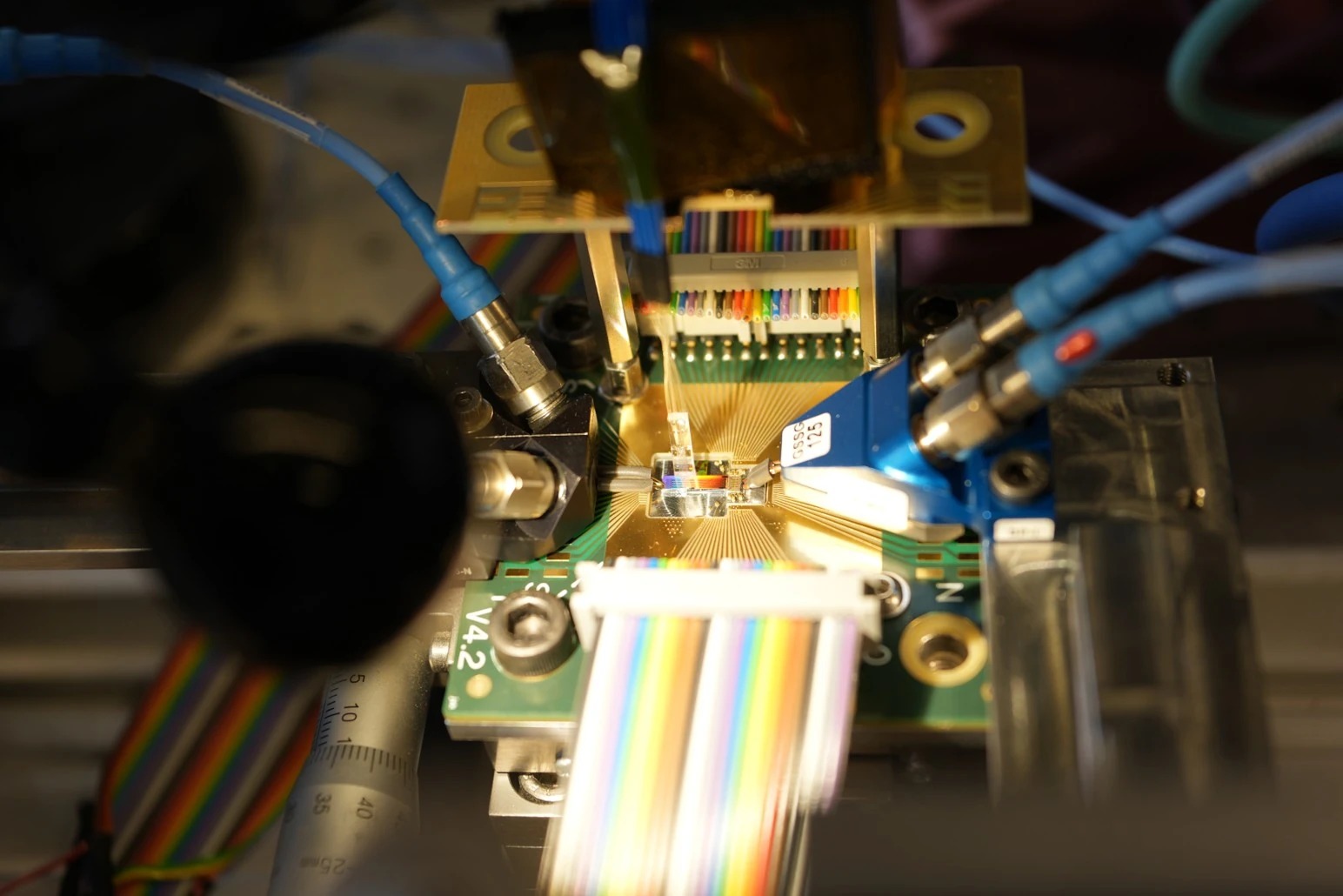
The research team has also achieved the first successful heterogeneous integration of a LiTaO₃ modulator onto a silicon photonic integrated circuit. Using the same microtransfer technology previously employed for lithium niobate, the researchers have ensured full compatibility with the entire wafer stack, allowing it to be integrated with other photonic components such as heaters, filters, and germanium photodetectors without any impact on performance.
Although these modulators are still relatively large at present, they provide a viable path for further expanding pluggable transceivers, as the constraints on space occupancy for such products are not as strict. Meanwhile, researchers are also exploring other device concepts to meet the future requirements of co-packaged optics for smaller sizes and higher integration levels. These solutions include compact, ultra-high-speed GeSi modulators that operate in the C-band, as well as emerging methods based on integrating III-V materials onto silicon photonics platforms.
To extend these heterogeneous integration methods to large-scale manufacturing, further work is still required. However, these results indicate that integrating electro-optical devices operating at frequencies exceeding 100GHz onto SiPho is a promising approach, and this is widely regarded as an essential capability for the next generation of optical interconnects that will support 3.2T pluggable modules and the infrastructure for AI drives in the future.
Fast and narrowband co-packaged optics ( CPO ): A key pillar of the optical interconnection roadmap
At this scale, a new set of constraints arises. Plug-and-play transceivers rely on very high baud rates and combine complex digital signal processing (DSP) to compensate for signal degradation. While this works well at the rack or data center level, for short-distance chip-to-chip optical interconnections in AI and machine learning systems, the high power consumption and latency caused by heavy DSP become increasingly problematic. On the contrary, these scenarios require inherently cleaner optical channels with extremely low bit error rates, so that each channel can operate without relying on excessive equalization or DSP overhead.
This transformation is precisely the reason that drives the adoption of fast and narrow-band co-packaged optics ( CPO ). In CPO systems, optical components are placed in close proximity to the silicon wafers or computing chips, reducing the electrical path from several centimeters in pluggable solutions to just a few millimeters or even less. By placing the electro-optical conversion point directly next to ASIC (within the same package), CPO significantly improves signal integrity, minimizes electrical losses, and reduces latency – without relying on high-power DSP. This makes CPO an attractive architecture for scaling up next-generation AI and high-performance computing systems.
Figure 3: Co-packaging of optics reduces the electrical path between the light engine and the host IC, thereby increasing bandwidth density and eliminating the need for digital signal processing, and thus enhancing energy efficiency. Source: imec.
However, as the early deployment of CPO began, integration complexity remained one of the core challenges of this technology. Unlike pluggable optical modules, whose optical components are largely self-contained, CPO requires close collaborative design and joint optimization, including photonic integrated circuits ( PIC ), electronic IC ( EIC ), switching ASIC , fiber coupling strategies, thermal management, and advanced packaging. Addressing this multidisciplinary challenge is one of the core objectives of the imec optical interconnection project.
In the CPO domain (also known as OIO2.5D), the main research objectives of imec include:
- Expand the capacity of the light engine from 1.6T and 3.2T to 6.4T, and ultimately reach 12.8T.
- Achieve a fast and narrowband channel rate of 400 Gbps, and increase bandwidth density to nearly 1 Tbps per millimeter.
- Integrate the complete optical stack – modulator, photodetector, coupler, fiber optic connections, and thermal solutions – into a manufacturable package.
Achieving these goals largely depends on advanced semiconductor packaging technologies to support the high-density integration of photonic and electronic components—such as 2.5D interlayer architectures, silicon through-hole technology ( TSV ), fan-out wafer-level packaging ( FO-WLP ), and an increasing number of 3D integrations realized through hybrid bonding—while also requiring the use of advanced ( III-V ) materials.
There is also the issue of light sources. Although the long-term goal is to integrate lasers directly onto photonic chips, the early CPO systems will still rely on external laser sources. This approach simplifies thermal management and alleviates the long-standing reliability concerns associated with operating lasers in high-temperature environments like ASIC. However, the trade-offs include the need for higher output power to compensate for light loss, more complex packaging, and the requirement for additional optical fibers and connectors to guide light into the package.
Achieved the first silicon-based EAM with a net transmission rate of 400Gbps per channel
In October 2025, imec announced a major advancement in next-generation optical interconnects: a C-band GeSi electroabsorption modulator ( EAM ) with a bandwidth of over 110GHz, capable of achieving a data rate of 400Gbps per channel.
This device utilizes the Franz-Keldysh effect, combining compact size, high speed, and low power consumption. Thanks to the foundation of GeSi, it can be seamlessly integrated into SiPho platforms that are 300mm in size and compatible with CMOS, providing a clear path for mass production.
This breakthrough reflects more than a decade of collaborative progress at both the device and system levels. At the device level, imec has optimized device size, doping schemes, and epitaxial growth processes. At the system level, robust PAM-4 IM / DD transmission schemes have verified sustained operation at a net rate of 400 Gbps per channel, proving that GeSi EAM technology already possesses practical usability for future high-channel-rate optical engines.
3D Integrated Optics ( OIO3D ): The Next Frontier
As AI and machine learning systems expand to include thousands of tightly interconnected accelerators, each accelerator is connected to adjacent processors over a distance of just a few millimeters through high-bandwidth memory stacks. This places even more stringent demands on optical interconnects. Over the next decade, these systems are expected to require bandwidth densities of nearly 10 Tbps per millimeter, energy efficiency far below 1 pJ/bit, and ultra-low latency (<100 ns). Such goals have surpassed what even advanced CPO architectures are capable of achieving.
To meet these requirements, optics must penetrate beyond the encapsulation and reach into the wafer stack itself. This is the foundation of 3D integrated optics. By compressing electrical paths to micron-level distances, OIO3D enables ultra-short, high-bandwidth, and high-energy-efficiency optical links, making optical networks between high-density chips possible.
Figure 4: By compressing the electrical path to a micron-level distance, OIO3D is able to achieve ultra-short, high-bandwidth, and high-energy-efficiency optical links, making optical networks between high-density chips possible. Source: imec.
Achieving 3D integrated optics requires overcoming several significant technical challenges. These challenges include scalable laser integration, the development of high-efficiency and high-bandwidth electro-optical devices (such as those based on GeSi, lithium niobate, lithium tantalate, indium phosphide, or barium titanate), as well as robust thermal management in high-density stacking environments. Equally critical are wafer-level ultra-precision bonding and alignment technologies.
OIO2.5D and OIO3D
As an evolutionary step from CPO, OIO2.5D achieves a balance between high-density photon integration and manageable packaging complexity by placing photonic chips and electronic chips side by side on a shared silicon interlayer. The photonic layer is integrated using die-to-wafer copper-based hybrid bonding technology, which enables ultra-short and low-parasitic electrical paths.
This architecture was initially designed for optical engines with a bandwidth range of 8-32 Tbps. It utilizes a channel rate of 32-64 Gbps and is optimized for low power consumption, without the need for DSP, in order to minimize latency and heat generation as much as possible. Wavelength division multiplexing (8-32 wavelengths per fiber) further increases the total bandwidth without the need to increase the number of fibers. The goal of this technical roadmap is to achieve a bandwidth density of 2 Tbps per millimeter, with an energy efficiency of nearly 2 pJ/ bit.
OIO3D represents the most advanced and ambitious vision for optical interconnection. Here, the photon layer is directly stacked above or below the computing silicon chips, forming a true chip-level optical network that compresses electrical paths to the micron level.
This method relies on the combination of die-to-wafer and wafer-to-wafer bonding to achieve vertical interconnections with extremely fine pitches. With this level of vertical integration, OIO3D aims to expand bandwidth capacity to tens of terabits per second or even higher, while setting an energy efficiency target of approximately 2pJ/ bit. In the longer term, it strives to operate at sub- pJ / bit levels.
A key research direction is wafer-level laser integration, which utilizes heterogenous III-V schemes such as quantum dots GaAs-on-Si. The pilot production lines under the EU's 'Chip Act' are actively exploring this direction to serve future large-scale photonic systems.
Integrating barium titanate on the 300mm SiPho platform
In January 2026, Veeco Instruments Inc and imec announced a process suitable for large-scale production of 300 million units, which allows barium titanate (BaTiO₃, BTO) to be integrated into silicon photonics platforms.
BTO possesses excellent electro-optical properties and can be used in high-speed, low-power modulators for applications ranging from optical transceivers to quantum photonics, LiDAR, as well as AR / VR. However, historically, it has been very difficult to introduce BTO on a large scale into silicon platforms due to limitations in cost, uniformity, and manufacturability.
Leveraging cooperation with imec, Veeco has recently delivered its first molecular beam epitaxy (MBE) cluster system designed specifically for 300mm wafers. This platform supports the growth of single-crystal BTO thin films on silicon, using both solid-state and hybrid MBE processes. Compared to traditional MBE solutions, it offers improved repeatability, material quality, and cost-effectiveness.
Timeline Overview
Looking at the development of optical interconnection, it is clear that different routes are advancing according to different timetables.
Pluggable optical modules have been deployed on a large scale worldwide, and now they have entered a phase that focuses on progressive technological optimization rather than fundamental breakthroughs. The roadmap continues to move forward towards 1.6T and 3.2T modules, and at the same time as new architectures are scaled up for production, plug-and-play solutions will still remain competitive in many application scenarios.
The encapsulation of optical technologies is also approaching a relatively mature stage. Key components are being transferred to trial production lines, with preparations for the supply chain and wafer-level services in place – although the industry continues to pursue higher bandwidths, faster channel speeds, and better energy efficiency. Large-scale deployment of CPO is expected to begin in 2027/2028.
3D integrated optics is still in an early stage of development. The current focus of work is on path exploration and the construction of device/integration toolkits. The first batch of concept validation demonstrators is expected to appear within three to five years, while broader commercialization is anticipated to be achieved over a period of five to ten years.
Bringing the next generation of optical interconnects to market
Through its optical interconnection research project, imec is developing key components for future optical transceivers, anticipating market demand several years in advance.
The advantage of imec lies in its being a true one-stop development environment, bringing together professional capabilities in silicon photonics, advanced CMOS, 3D integration, material research, and system-level modeling. This breadth enables researchers to explore new concepts more quickly than in large-scale manufacturing environments, thus achieving shorter development cycles and having the freedom to try unconventional integration paths. The project also benefits from imec's cross-technology optimization (XTCO) strategy, which promotes expansion across different technical fields.
A key accelerator is the close collaboration between the imec Optical Interconnect Research Team and IC-Link – the semiconductor manufacturing backbone of imec. The early research of imec focused on path exploration and prototype development, while IC-Link helped to advance the technology towards greater maturity by optimizing process flows, enhancing manufacturability, establishing testing strategies, and coordinating with a broader supply chain. Through IC-Link, industry partners can also leverage imec's 200mm and 300mm iSiPP silicon photonics platforms to access and evaluate these technologies, providing a pathway from early innovation to industrial deployment.
In addition to IC-Link, imec also maintains close interaction with industry partners through various collaboration models. These models include guidance-based projects (where imec explores emerging technologies together with partners), targeted bilateral projects that address the specific needs of certain partners, as well as long-term core partnership relationships. At the same time, imec also works closely with equipment suppliers to enable early verification of advanced tools and technological capabilities before they are commercialized.
These interactions collectively ensure that the optical interconnection research of imec is always rooted in real system requirements, while also accelerating the transformation of advanced technologies into market-ready solutions.
Peter Ossieur obtained a Master's degree in Electrical Engineering from the University of Ghent in Belgium in 2000 and a Doctoral degree in the same field in 2005. From 2005 to 2009, he worked as a postdoctoral researcher at the University of Ghent, after which he joined the Tyndall National Research Institute, where he was promoted to Senior Researcher. His research interests include electronic integrated circuit design and optical transmission systems. In 2017, he joined the imec-IDlab at the University of Ghent. Today, he is the head of imec, XTCO Fabric, and, and Optical Interconnect, and also serves as an adjunct professor at the University of Ghent. Peter Ossieur is also a member of the ISSCC Wired Communications Subcommittee.
Imene Jadli