









IT News on November 4th: NVIDIA published an article on November 3rd stating that artificial intelligence is pushing semiconductor wafer factories into the "AI defined factory" phase: by accelerating simulation, learning-based physical models, AI intelligents, and digital twins, design, testing, and production decisions in chip manufacturing are being significantly accelerated.
Accelerated simulation (accelerated simulation) refers to the use of technologies such as GPU, parallel computing, and AI intelligent agent models to compress the process of engineering simulation, which traditionally relies on CPU, from several hours or days to just minutes or even milliseconds. In semiconductor manufacturing, it enables engineers to test process plans more quickly and predict defect risks without having to conduct expensive and time-consuming real-line experiments first.
As cited in a blog post by IT, with the increasing demand for advanced chips, manufacturing processes have become increasingly complex, and the margin for error in terms of yield and process quality continues to shrink. Traditional production line experiments are both slow and costly; engineers often need several days to analyze process changes, material reactions, or the root causes of defects. The value of AI lies in allowing engineers to compare different options more quickly and identify risks in a virtual environment before undertaking actual experiments.
The goal of accelerated simulation is to obtain sufficiently reliable “virtual experiment” results more quickly before actual manufacturing, thereby reducing trial and error, improving yield, and lowering costs.
A learning-based physical model ( Learned physics models ) refers to a model that utilizes machine learning to learn physical laws from high-precision simulations, experiments, or production line data. It learns the mapping relationships between variables such as temperature, pressure, materials, electromagnetic fields, and plasma, thereby enabling rapid prediction of complex physical processes. In its reports on semiconductor manufacturing, NVIDIA considers it one of the key technologies for accelerating wafer factory simulations and decision-making.
Digital twins (Digital Twin) refer to dynamic digital replicas of physical objects, systems, or processes created in a virtual environment. They are not just static 3D models; they can receive real-time or historical data, simulate operating states, predict outcomes, and support a decision-making approach of "testing first in the virtual world before implementing it in the real world." In NVIDIA's reports on semiconductor manufacturing, digital twins are used to build virtual models of entire wafer factories, helping engineers identify bottlenecks, verify layouts, and operational strategies before production begins.
In specific cases, multiple physical field simulation software COMSOL utilize NVIDIA cuDSS to increase the simulation speed related to semiconductor manufacturing by up to 10 times; Siemens has integrated cuLitho into its Calibre lithography software, achieving a maximum speed increase of 17 times for key simulation tasks.
After integrating cuDSS, the Ginestra platform of Application Materials Company (Applied Materials) is up to 10 times faster than the solution that uses only CPU. Moreover, its ACE combined with multiple physical field platforms can achieve a shape simulation acceleration of up to 35 times with the help of PhysicsNeMo.
AI can also reduce the need for repeated simulations. For example, the modeling of plasma behavior used in semiconductor etching is complex and costly; Lam Research demonstrates that PhysicsNeMo can predict plasma behavior in milliseconds, while a complete simulation may take several days.
In the past, engineers needed to wait for long periods of time for simulations, experiments, or data analysis to determine whether a certain chip manufacturing scheme was feasible. With the introduction of AI for accelerated simulation, learning-based physical models, and AI intelligent agents, many analysis tasks that previously took days can now be completed in just minutes.
NVIDIA cited in the report that Advantest uses NeMo Switchyard AI agents to automatically select the appropriate AI models, compressing tasks that originally took hours into just a few minutes.
In advanced wafer factories, the problems engineers face are often not simply about querying data; they usually require judgment:
- Whether a certain etching parameter will damage the wafer;
- Whether a change in material or process will affect the yield rate;
- Whether the defect comes from the equipment, materials, or process conditions;
- Among multiple candidate solutions, which one is most worthy of being verified in a real production line?
Traditional processes typically involve high-precision physical simulation, result analysis, and comparison of options in sequence, and sometimes actual experiments are also arranged. A complete simulation can take several days, making it difficult for engineers to quickly explore a large number of alternative solutions.
AI can help engineers narrow down the possibilities and identify high-risk solutions in advance, but key process changes still require high-precision simulation, experimental verification, and professional review by engineers. AI liberates engineers from having to wait for long periods for calculation results, allowing them to focus their time on making judgments, verifications, and optimizations; although the waiting time in the decision-making process has been reduced, the professional responsibility and final approval still lie with the engineers.
In the past, it was like doctors had to wait for a complete set of test reports before they could make a preliminary assessment of a patient's condition; now, AI is equivalent to quickly providing multiple screening results and possible causes, allowing doctors to immediately decide which key tests to prioritize. The speed has increased, but the final diagnosis and treatment decisions are still the responsibility of the doctors.
More importantly, Applied Materials is building a digital twin of the entire wafer factory based on NVIDIA Omniverse. This allows for the simulation of material flow in a virtual environment, the identification of bottlenecks, and the verification of layout and operational strategies before deciding whether to implement them in the actual production line.
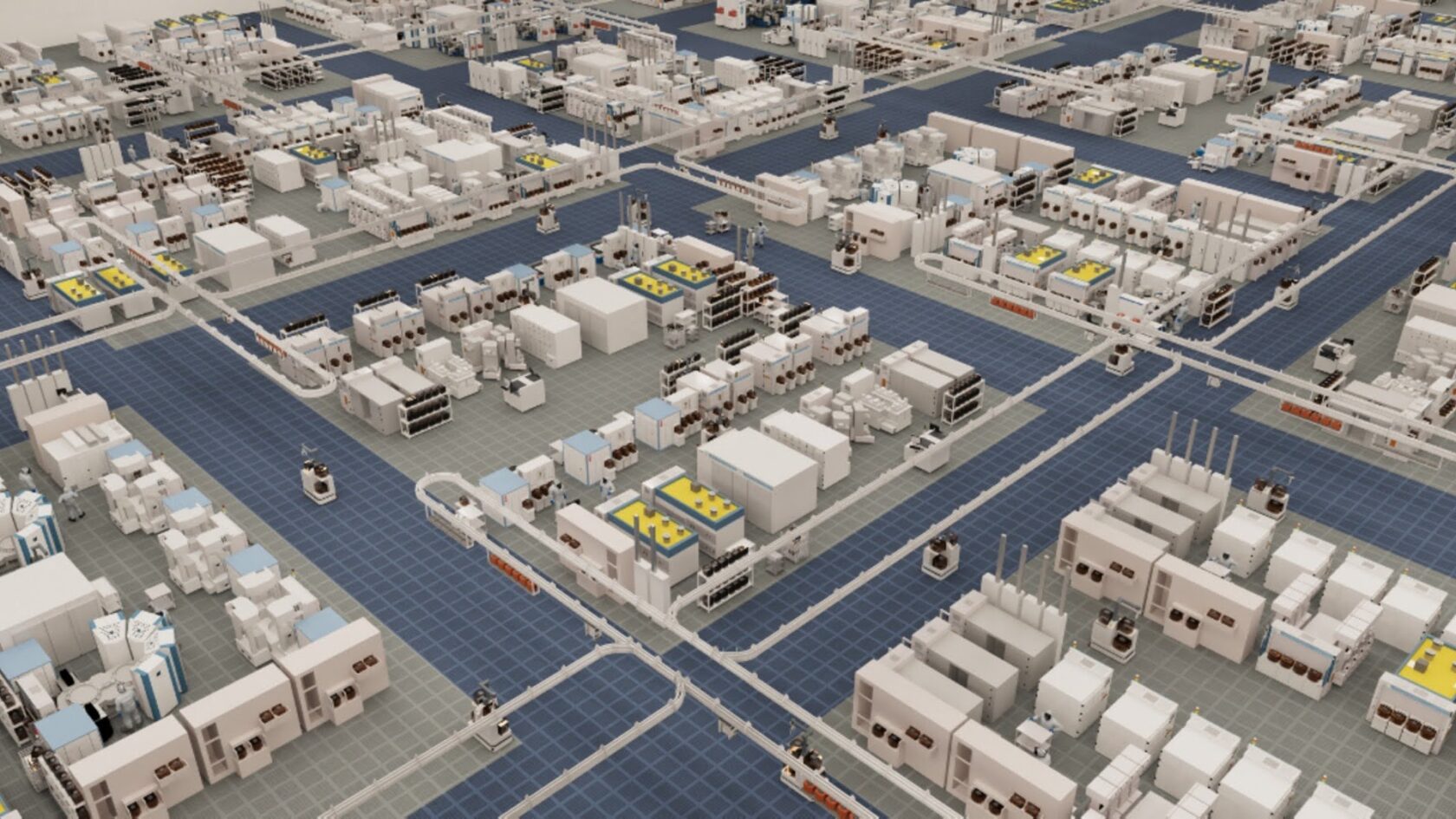
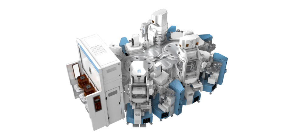
NVIDIA claims that this closed-loop system will enable factories to learn from each production cycle and take action earlier; engineers will still be responsible for professional judgment and final decisions, but the time required to wait for answers will be significantly reduced.