












News from the IT Home on October 14th: Today, IBM and Siemens announced a new research collaboration aimed at advancing the nanostacked (nanostack) transistor architecture that IBM announced earlier this year.
According to an official press release from IBM, this collaboration will combine IBM's leadership in the field of semiconductor device innovation with Siemens' expertise in electronic design automation (EDA), process simulation, lithography optimization, and advanced manufacturing software, in order to accelerate the development of nanostacking technology.
According to the introduction, the cooperation between the two parties includes developing advanced virtual models of nanostacks in order to model performance, optimize designs, and solve manufacturing challenges before chip production.
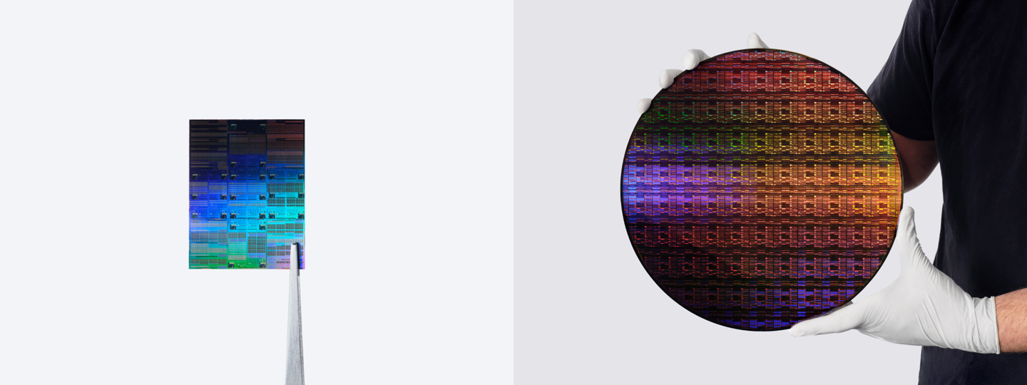
IBM first released the nanoscale stacking architecture in June of this year, calling it the industry's first known three-dimensional nanosheet design. Unlike the current approach of laying transistors flat on a two-dimensional plane and continuously reducing the spacing between them, nanoscale stacking arranges transistors vertically in a staggered pattern, allowing for more transistors to be packed into the same area.
Under the current 7-angstrom (0.7 nanometers) node, this design can integrate nearly 100 billion transistors within an area the size of a fingernail, with a density approximately twice that of the 2nm test chip released in 2021 by IBM. This design also allows for the use of different material combinations in each stacked layer, thereby independently optimizing the performance and power consumption of each transistor.
IBM Previous research results have shown that, compared to 2nm nodes, the nanostack architecture can improve performance by up to 50% at the same power consumption, or reduce power consumption by up to 70% while maintaining the same performance.
At the VLSI 2026 seminar, IBM also reported that nanostacking achieved a 40% reduction in size on SRAM (Note from IT: static random access memory), which is of great significance for the high-bandwidth memory required by AI workloads.
IBM Research Director Jay Gambetta stated at the press conference: "We are not just making transistors smaller, but re-inventing the way chips are built to provide significantly higher performance and energy efficiency."
IBM, Vice President of Silicon Technology Research and Development, stated: "Nano-stacking is an scalable transistor platform designed to transition device miniaturization from two dimensions to three dimensions. It represents a new paradigm in the semiconductor industry and is also the logical path to miniaturization required to support AI and other emerging technologies over the next decade."
Siemens' Ankur Gupta, the Vice President of Combined Operations, stated: "To advance semiconductor miniaturization to the era of atoms (em), it is necessary to achieve close collaborative optimization between device physics, EDA design and manufacturing software, and the manufacturing process itself."
IBM once stated that it is estimated to take about five years for the first products based on this technology to be put into production by partners. This collaboration with Siemens is precisely designed to bridge the gap from the laboratory to the factory.