















On October 23rd, well-known tech podcast host Dwarkesh Patel released his latest special episode. He spent two days visiting Intel's wafer factories and research laboratories, where he had conversations with five technical leaders. The topics ranged from ring gates, backside power supply, CFET, to Intel's collaboration on the project with Elon Musk Terafab.
These discussions point to two conclusions. Chips in 2045 will continue to evolve towards three-dimensional stacking: transistors, interconnections, and the connections between chips will all be stacked upwards. However, each new structure takes about a decade to overcome challenges related to heat dissipation and integration. Engineers themselves only have a visibility of about four years regarding the technological path ahead. A more immediate constraint is related to equipment: The host mentioned that AI computing power has been tripling every year for the past decade. Intel’s CTO estimates that the current global equipment is only sufficient to double the production of advanced-process wafers.
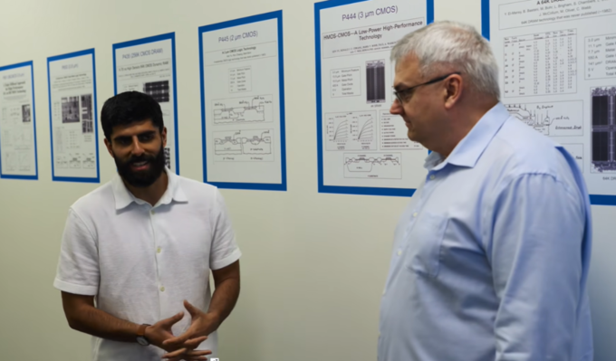
Intel R&D Director: Chips in 2045 will grow larger, and heat is an unavoidable issue
Chips rely on transistors for computation. Transistors are miniature switches, with their on and off states corresponding to 1 and 0 respectively. When a voltage is applied to the gate of a transistor, the channel beneath it becomes conductive; when the voltage is removed, the channel closes.
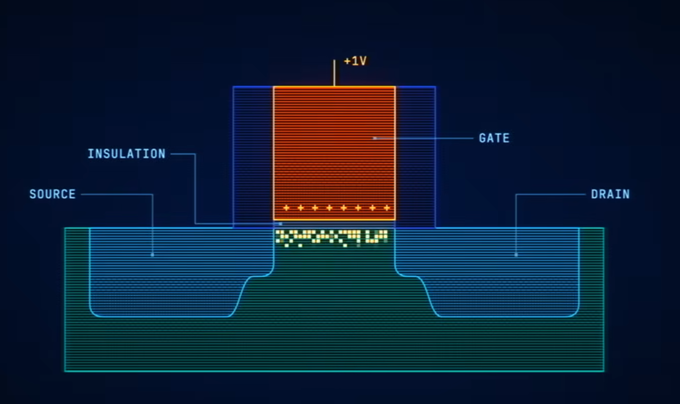
After the device is scaled down, the channel cannot be sealed tightly, and current will leak through. The solution is to have the gate control the channel from more sides: planar transistors only press down on the top, while FinFET turns the channel into thin fins, surrounding it on three sides. The gate then encircles the channel, cutting it into suspended thin strips, with each strip being wrapped completely by the gate.
Chris Auth, who is responsible for the development of existing mass production processes at Intel, said that the gate-all-around (GAA) structure has been known to be the ultimate goal since the 1990s: "Gate-all-around is truly the ultimate transistor technology." The previous steps were not skipped; from strained silicon to high-K metal gates to FinFET, one doesn't proceed with these technologies until it's absolutely necessary.
The next step is CFET: The transistors in the circuit are of N-type and P-type, appearing in pairs. Today, they are placed side by side. CFET involves stacking them one on top of the other, which allows for twice as many transistors in the same area, but the trade-off is that interlayer wiring becomes more difficult, and heat dissipation becomes more challenging.
Chris believes that by 2045, the design will become even more radical. "Now you're looking at a transistor that's suspended within interconnections, and you can't help but wonder: why not combine transistors with interconnections, and add more transistors and more interconnections? Memory chips have already achieved this, and NAND flash memory already has a three-dimensional structure. He thinks that DRAM will inevitably follow this path as well."
Thermal dissipation is the biggest limitation. He identifies three factors that limit computing power: how quickly the switches can be activated and deactivated, how much power they consume during these processes, and how effectively the heat can be dissipated. The issue of heat becomes even more prominent with three-dimensional devices: “This will be a limitation, and it always will be a limitation, but we are capable of solving these problems.” As for when these solutions will be implemented, he is quite cautious: “Our visibility for technological advancements is about four years. After those four years, I think we could continue to make further progress for another four years. But if we talk about ten years, it’s hard to say what the situation will be like then.”
On top of the transistors, there are another ten or so layers of metal wires that need to be stacked to connect them into a circuit. This layer is known as interconnect, and currently, copper is used for this purpose. Researchers in the laboratory, including Jack Kavalieros, are exploring the possibility of using ruthenium as a substitute for copper. With copper wires, a layer of pad material must be laid down first before they can be firmly attached; the finer the wire, the larger the proportion of the cross-section that the pad material occupies. Ruthenium, on the other hand, can be etched directly without the need for a pad. They say, "At those very fine dimensions, if we can replace the resistance of the pad material with that of ruthenium, then ruthenium begins to have an advantage." The intersection points are spaced at approximately 20 nanometers apart. They also point out that although cobalt was chosen for the previous node, now copper has been adopted again; "Cobalt was the leading option at that time, now it's copper again, and in the future, it might be ruthenium."
The connection between chips is explained by Tyler Osborn, the director of the Advanced Packaging Technology Development Department. The program's narrator points out a contradiction at the beginning: although the chip area doubles, the edge length only doubles as well, yet data exchange between chips is conducted through these edges. During AI operations, the speed of data transfer often determines the overall speed more so than the computation itself.
One of the solutions is hybrid bonding: by skipping the solder joints and directly aligning, pressing, and heating the copper interfaces of two chips together, the contacts can be arranged more densely. Tyler provides a set of figures: 15 years ago, the interconnect pitch was between 130 and 150 micrometers; today, in mass production, Foveros has achieved 25 micrometers, and in laboratories, it has already been reduced to below 10 micrometers. This year, at the IEEE ECTC conference, there were papers presenting reliability data for hybrid bonded devices with a pitch of 0.45 micrometers. His comment was: “I see a very long runway ahead here.”
The new structure didn't enter mass production until ten years later; Intel set quotas for innovation.
FinFET It was verified in the laboratory in 1989 and mass-produced in 2011. The ring gate technology was verified in 1988 and wasn't mass-produced by Samsung until 2022. This is the timeline provided by the program. In between, it took about 2,000 processes to achieve stability, and it was necessary to be able to repeat these processes in batches on wafers (the round silicon slices from which chips are cut) every week, while also meeting the yield requirements (the proportion of qualified chips).
Intel's lesson came from 10-nanometer technology (a generation of manufacturing process, referred to as a node in the industry). Chris recalls that at that time, the scaling speed far exceeded historical levels, and it had to be accomplished without new tools, “which placed a great burden on the processes and engineers.” He believes that the technology that should have been postponed the most was EUV (extreme ultraviolet lithography): “When we started working on 10-nanometers, the conclusion was that EUV was not ready yet.” EUV used light with a wavelength of 13.5 nanometers to print circuit patterns onto wafers; the shorter the wavelength, the finer the lines that could be printed at one time. The program’s narration explains the outcome: 10-nanometer production was originally scheduled for 2016, but it didn’t begin until 2018; TSMC started mass-producing EUV in 2019, while Intel’s first EUV process did not produce any products until 2023.
Intel's external customer decisions for the 14A are underway, and customers value predictability in progress. Chris summarizes: "What we've learned is that you shouldn't try to do too much innovation within a single node, because the more innovation there is, the higher the complexity." To address this, Intel has established a 'phase gate': new technologies must pass through a trial phase before entering development, and they must meet standards in terms of yield, defects, and performance; if they don't, they are pushed forward to the next generation.
The same pragmatism is also evident in the meeting rooms of wafer factories. At the Hot Topics meeting, when information is incomplete, Kevin Fischer has to make decisions: “One thing you’ll learn is that you will never have a complete dataset. If you wait for a complete dataset, you’ll have waited too long, and it will be too late by then.” What he needs to determine is “how much risk we are willing to take.”
The example he cited was "extensive nodules." Extensive growth refers to the formation of new crystals layer by layer on the surface of the wafer; when this happens locally, it can result in protrusions that cause short circuits between adjacent areas and render transistors inoperable. The team worked in a highly parallel manner, testing multiple solutions simultaneously—both adding cleaning processes to remove the nodules and seeking to identify their root causes. The highest priority batch, designated as HotBox, had priority on every piece of equipment. Kevin said, "It's like reserving a lane on the highway for this experiment only; everyone else has to give way." However, the cost of this approach was that it would slow down the entire factory, which is why the staff were reluctant to resort to this measure.
In the research laboratory, a new structure starts with a “short process” prototype: only a few key steps are carried out first, and once these are accurately measured, they are then combined to form a more complex device. For example, for CFET, a simplified version with a strip at the top and one at the bottom is created first; it may not even be superior to the current parallel nanostrips, but it allows for the verification of wiring issues after they are stacked. The elimination of materials is also straightforward; a new material might be ruled out simply because it “doesn’t stick,” or the gases used in subsequent processes could alter its properties. “If we can’t find a way to control that, it’s a dead end for us.”
Intel CTO: We need 3 times the computing power, but the devices only provide 2 times.
The host mentioned that ASML delivers less than 100 EUV lithography machines per year, which are distributed to Intel, TSMC, and SK Hynix, among others. Intel CTO Pushkar Ranade acknowledges this as a limitation, but also stated that “EUV or ASML is not the only bottleneck” and “we are seeing severe shortages of all equipment.” Once a manufacturing process is determined, the equipment is locked in: “We cannot just switch to a different machine for the same process.” His strategy to mitigate this is to try to keep the equipment versatile between different nodes; “From 18A to 14A, perhaps 80% of the equipment can be reused.”
When the host asked if there were enough devices globally to increase the production of advanced process wafers by 10 times, he replied, "10 times is not possible, maybe 2 times would be feasible." The host pointed out that in the AI industry, computing power has been increasing by 3 times each year over the past decade. Pushkar stated that unless the entire supply chain increases production as well, it will not be possible to boost output. The host summarized, "Output can be increased within 12 months, but by 2030, it will not be much higher than the current projections." Pushkar added that the cycle for equipment orders is "18 months before delivery," which means we would be entering 2028 by then, and to build new factories, "it would basically have to wait until the end of this decade."
Behind this is the cost structure of the foundry industry. Pushkar says, "After a wafer factory is built, about 80% of the costs are fixed." The initial investment in infrastructure such as circuits and stations incurs expenses, but adding one more passenger hardly increases costs at all; therefore, every additional percentage point in utilization directly translates into revenue. He also attributes the concentration of the industry to this factor: forty years ago, there were twenty foundries, but now only three remain.
To catch up with TSMC, he believes what needs to be improved is scale: “What we need to pursue is scale.” “If you’re talking about technology, I think we’re already there; perhaps we fall short by a few percentage points in terms of performance, power consumption, or area density.” In response to the comparison cited by the host, which includes SemiAnalysis, he said, “First of all, I don’t agree with your benchmark tests.” His standard is punctuality: it’s okay to fall short by a few percentage points, “but you must be punctual.”
In terms of capital expenditure, the host mentioned that TSMC plans to spend around $50 billion this year, while Intel plans to spend about $20 billion (TSMC has already raised its capital expenditure forecast for 2026 to $60 billion to $64 billion). Pushkar believes this is unfair, as TSMC essentially serves as a foundry for almost everyone, whereas Intel uses its own facilities for most of its production. As the number of external customers increases, Intel's expenditure is also set to rise.
Terafab is an example of external pressure. Pushkar quotes Musk's thoughts: “We either build Terafab, or we won't have chips at all.” The host pointed out that tools are the bottleneck, and the total amount of silicon in the world will not increase as a result; Pushkar responded that electricity, water, and consumables can be expanded, but “tools cannot.” He also said that the cost of building a wafer factory doubles every 4 to 5 years, and a single High-NA lithography machine along with its supporting equipment costs about 400 million dollars; this curve cannot extend indefinitely. He proposed a thought experiment: if people in a research wafer factory were allowed to eat hamburgers and smoke cigars, to see what would happen to the yield rate. He admitted that no existing manufacturers are willing to do this: “This is an industry that dislikes risk.”
At the end of the interview, the host suggested that Intel make large-scale commitment to purchasing tools, similar to how NVIDIA locked in its memory supply. Pushkar replied, "If we had known what we know today, we would have invested more about a year ago. Knowing the current situation, I think we would invest even more." He also mentioned selling their flash memory business, saying, "Obviously, in hindsight, that was not the wisest decision." He believed that the shortage in memory supply was even greater than that in computing power.
For the same High-NA lithography machine, Intel and TSMC come to two different conclusions.
High-NA is an upgraded version of EUV. The focal aperture (numerical aperture) of the lens has been increased from 0.33 to 0.55, allowing for approximately 1.7 times smaller feature sizes per exposure. When the patterns are too dense, the machine cannot print them all at once, and they have to be printed in two or three separate sessions. Each session consumes machine time and also increases the chance of defects. The narrator did the math: a EUV costs about 200 million US dollars, while High-NA is about twice as expensive. Whether it's worth it depends on how many fewer exposures are required.
Chris said that two companies came to different conclusions about the same device, and the reason lies in the architecture. "We use backside power supply, which means that the spacing requirements on the front side can be relaxed." With backside power supply, the thicker power cables are moved to the back of the wafer, leaving only thin signal lines on the front side, thus providing more space for routing. High-NA believes that TSMC, which does not use backside power supply, has to maintain tighter spacing, which High-NA finds impossible to achieve, so they have to continue using double exposure techniques. EUV "That's not very helpful for them, but it is very helpful for us." However, this is just the view from Intel's perspective.
What the market is concerned about at this moment is cost. TSMC Chairman Wei Zhijia stated at the shareholders' meeting in June that the reason High-NA has not yet been mass-produced is purely due to cost. In September, there were reports that TSMC had agreed to use High-NA in mass production starting from 2030. Intel has reserved it as an option for 14A, and Chris said that they would discuss it with each customer individually: "It has value, but also comes with increased complexity."
Intel now also manufactures chips (under contract) for other companies and provides customers with process design kits (PDK), specifying what can be manufactured with that process and the rules to follow. (Chris) acknowledges that Intel has only focused on its own products for decades and did not have a formal (PDK) process; "The 18A process initially did not have a (PDK)," which was only added after customer feedback, while the 14A process has been produced according to these standards from the beginning.